
CT inspection for electronics and semiconductors
Solder joints, vias, wire bonds and hybrid bonds are small, dense and hidden inside the part. Voxray QRT reconstructs CT scans of electronics with fewer metal artifacts, supports laminography for full boards and resolves submicron structures in advanced packaging.
Why electronics are hard to scan
X-ray CT shows the inside of an electronic assembly in 3D without cutting it. 2D X-ray inspection overlays the top and bottom of a board in a single image, and a cross-section shows a single plane and destroys the part.
Electronics combine the worst cases for CT reconstruction. Solder, copper and tungsten sit right next to plastic, silicon and laminate, so beam hardening and metal streaks cover exactly the regions you need to inspect. Boards are wide and flat, so a circular scan sends rays through their full width. And the features get smaller with every package generation, so scans run at high magnification with few photons and a lot of noise.
Where QRT makes the difference
Multi-material parts: plastic, adhesive and voids next to solder and copper stay visible.
Full boards: laminography and robotic CT scan PCB assemblies that don't fit a circular scan.
Advanced packaging: submicron voids and misalignments in hybrid bonds and redistribution layers.
Shorter scans: noisy, fast scans still give clean volumes with denoising.
Typical inspection tasks
What CT shows in each task, and what makes it hard for conventional reconstruction.
Solder joint voids
What CT shows: Size, number and position of voids in every joint of BGAs, QFNs and power modules, in 3D instead of overlaid in one image.
What makes it hard: The voids sit inside dense solder, where beam hardening and streaks from neighboring joints blur their edges.
Head-in-pillow and non-wetting
What CT shows: Whether a BGA ball is actually connected to the paste on the pad, or only touches it.
What makes it hard: The gap is only a few micrometers wide and lies between two dense parts, so it needs high resolution and few artifacts.
Connectors and overmolded parts
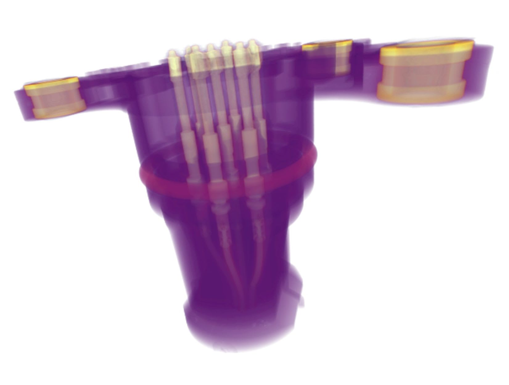
What CT shows: Voids, gaps and particles in the plastic between metal pins and inserts.
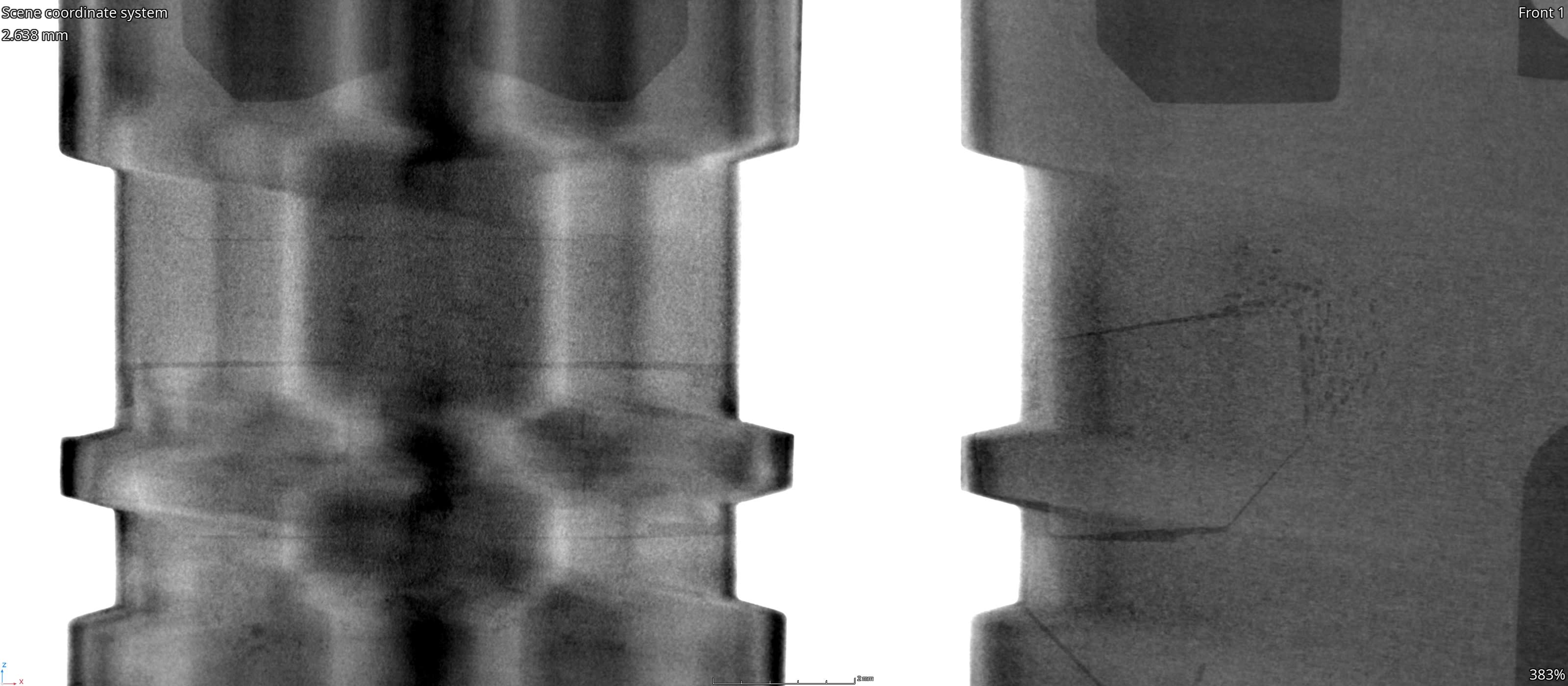
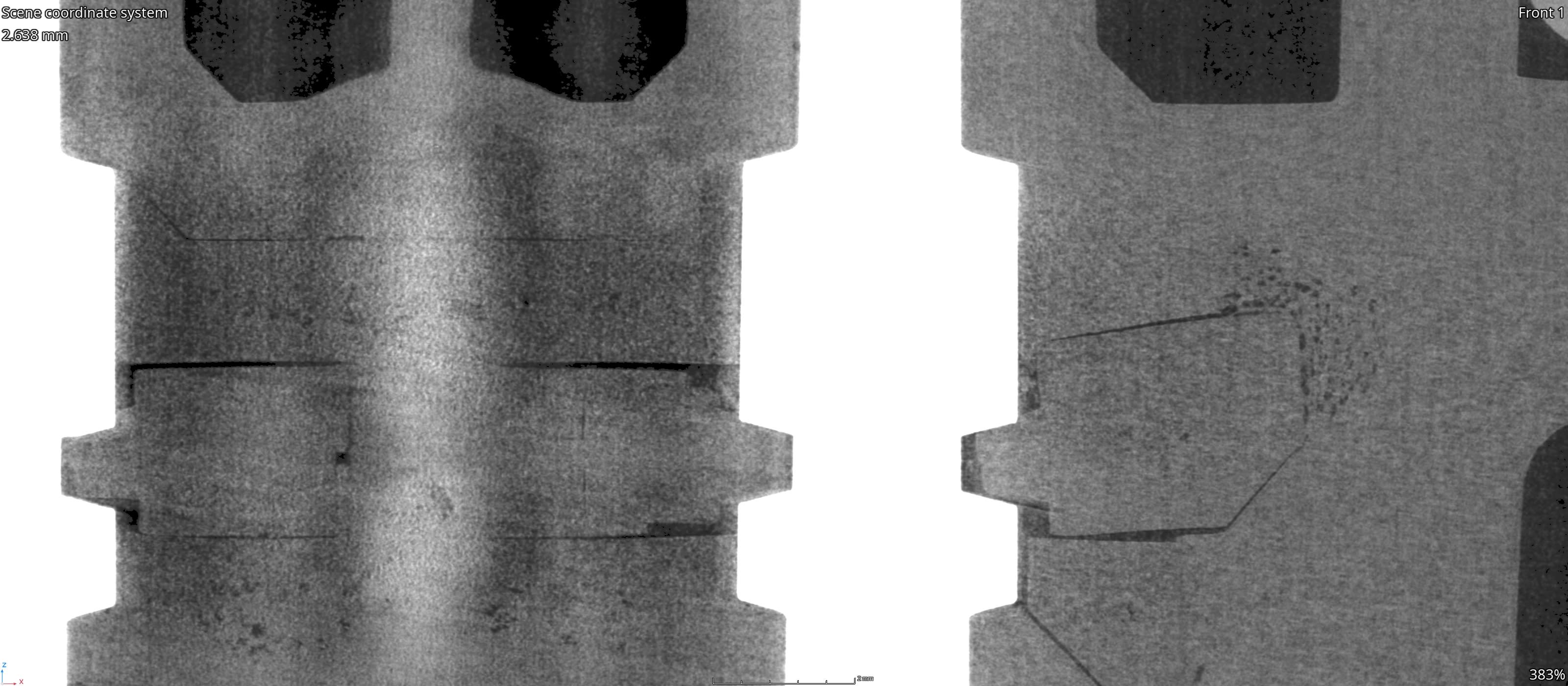
What makes it hard: Metal streaks cover the plastic. In our connector case study, filtered backprojection hid voids that QRT resolved.
Wire bonds and lead frames
What CT shows: Wire sweep, broken or lifted bonds and voids in the mold compound of packaged chips.
What makes it hard: Thin wires run next to the dense lead frame and die attach, which cause streaks across them.
Vias, traces and delamination
What CT shows: Barrel cracks in vias, the layer structure of the board and separations between layers.
What makes it hard: Large, flat boards are a poor fit for circular CT. Laminography scans them, but needs a reconstruction that supports it.
Hybrid bonds and microbumps
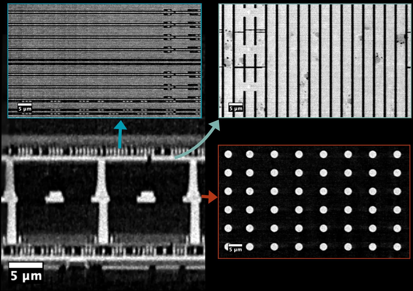
What CT shows: Submicron voids, density variations, misalignment and delamination in advanced semiconductor packaging.
What makes it hard: Needs nano-CT at the limit of the photon flux. Scans take hours, and the sample drifts during the scan.
Before and after
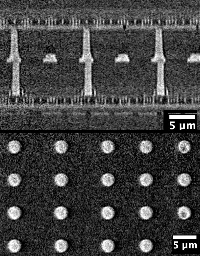
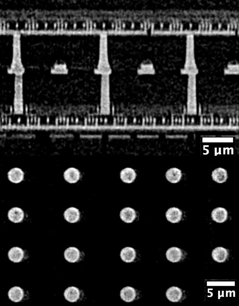
Conventional reconstruction compared with Voxray QRT on scans from our case studies. Drag the slider to compare.
Why QRT for electronics
QRT models the polychromatic X-ray spectrum and the physics of the measurement. Solder, copper and the material around them are reconstructed in one model, so the streaks of filtered backprojection don't form in the first place.
The same algorithm reconstructs circular scans, laminography and robotic CT, and corrects geometry errors and sample drift for every projection. That covers everything from a full motherboard to a submillimeter pillar cut from a processor.
Fewer metal artifacts
Voids, gaps and plastic next to solder, copper and pins stay visible.
Laminography for boards
Tilted axis, detector shifting and robotic laminography for large, flat assemblies.
Drift correction
Geometry errors and sample drift are corrected during the reconstruction, which matters for long nano-CT scans.
Your inspection system
QRT reads the raw data of all major manufacturers, including Comet Yxlon, Nikon, Nordson, Viscom, Waygate and Zeiss.
Case studies from electronics and semiconductors
From advanced packaging to full boards and connectors.

Frequently asked questions about CT in electronics
Why use CT instead of 2D X-ray inspection for electronics?
2D X-ray overlays everything along the beam in one image, so the joints on the top and bottom of a board and the voids inside them overlap. CT separates them in 3D and shows each joint and each layer on its own.
Can CT inspect a complete PCB assembly?
Yes, with laminography or robotic CT, which scan wide, flat boards at an angle. In our motherboard case study, QRT reconstructed an entire motherboard at 30 µm from a robotic laminography scan.
Why do solder and copper cause artifacts in CT?
They absorb far more X-rays than the plastic and laminate around them. Beam hardening, photon starvation and scatter make the data along these rays inconsistent, and filtered backprojection spreads the errors across the slice as streaks.
Can CT resolve hybrid bonding structures?
Yes, with nano-CT. In our hybrid bonding case study, QRT resolved 3 µm bonding pads and submicron voids at a resolution of 239.8 nm, close to the 200 nm limit of the 400 nm X-ray spot.
Does QRT work with my X-ray inspection system?
QRT reads the raw projections of all major CT manufacturers, including Comet Yxlon, Nikon, Nordson, Viscom, Waygate and Zeiss. Custom-built systems can use the open Voxray projection format.
Can I test QRT on my own scans?
Yes. Request a free trial and reconstruct your own datasets on your workstation, or choose the reconstruction service and send us a dataset to reconstruct for you.
Related topics
Inspect your electronics with QRT
Reconstruct your own scans of boards, connectors or packages in a free trial, or talk to us about your inspection task.